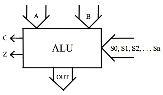
It is active whenever the most recent ALU calculation produces a zero result. Programs often need to branch when a zero result occurs. In order for programs to take such events into account, these events must be stored. Also, there must be a way for a program to determine whether the condition occurred (1 for yes or 0 for no).
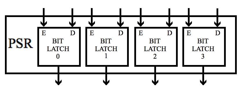
The storage mechanism for these bits is the Processor Status Register (sometimes called the PSR). Here is a diagram of a four-bit processor status register:
The following device selects as output one of the four bits of the processor status register. It is called a multiplexer. This particular multiplexer is called a 2 to 4 multiplexer because it has two select inputs to determine which of four other inputs will become the output. Notice that it utilizes a 2 to 4 decoder to select one of four buffers to enable.

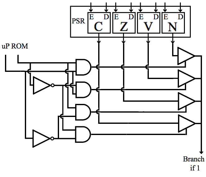
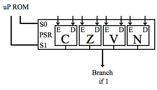
If a microprocessor of the type described so far is to be able to branch when the last calculation of the ALU produces a zero result, an address different from the one in the program counter must be made ready by the Branch if 1 output. The figure below replaces the bit latch numbers with the names of status bits. One of them is Z. It equal to is 1 if the most recent calculation resulted in zero.
There are several ways to implement a multiplexer with logic gates. Regardless of its internal design, a more compact representation such as the figure below is often useful. The abbreviation MUX is employed in such a case.
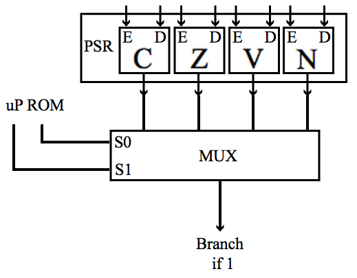
In this case, the multiplexer has two inputs, S0 and S1, that are from the microprogram ROM. The purpose of the functional unit is to create a signal that determines which of two addresses will be placed on the address bus in order to read the next instruction.
As in the above figure, the processor status register may be represented as including the multiplexer that selects the bit that is to be active.
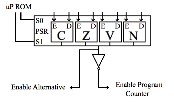
If the output of the processor status register is 0, the usual process of advancing the program counter or updating it is enabled. If the output of the processor status register is 1, an alternative address is enabled.
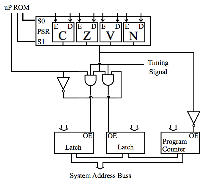
The figure above diagrams three sources of address bus numbers, each having tri-state outputs enabled in such a way that only one source writes onto the address bus at any given time. There are two triple-input AND gates that are used to enable one of two output sources. A signal from the microprogram ROM assures that the output of only one of these AND gates is at logic high. A timing signal keeps both these outputs low until it is time to change the number on the system address bus. If the output of processor status register is 1, both of these AND gates are set to enable the source chosen by the microprogram ROM.
The sources of data and timing used by the three devices providing numbers to the system address bus are not determined in this diagram.
This four-bit processor status register example holds information about the last calculation made by the ALU, but other possible status bits could indicate conditions not determined by the ALU. The status bits shown are C for the carry bit, Z for the zero result bit, V for the overflow bit, and N for the negative result bit. This bits are often called flags. For instance, V his often called the overflow flag. The meaning and use of V and N are tied to the particular way hardware adders are used to perform subtraction. Although this is almost universal, it may not always be so.
Contact
https://www.futurebeacon.com/jamesadrian.htm