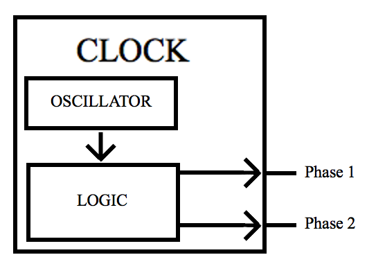
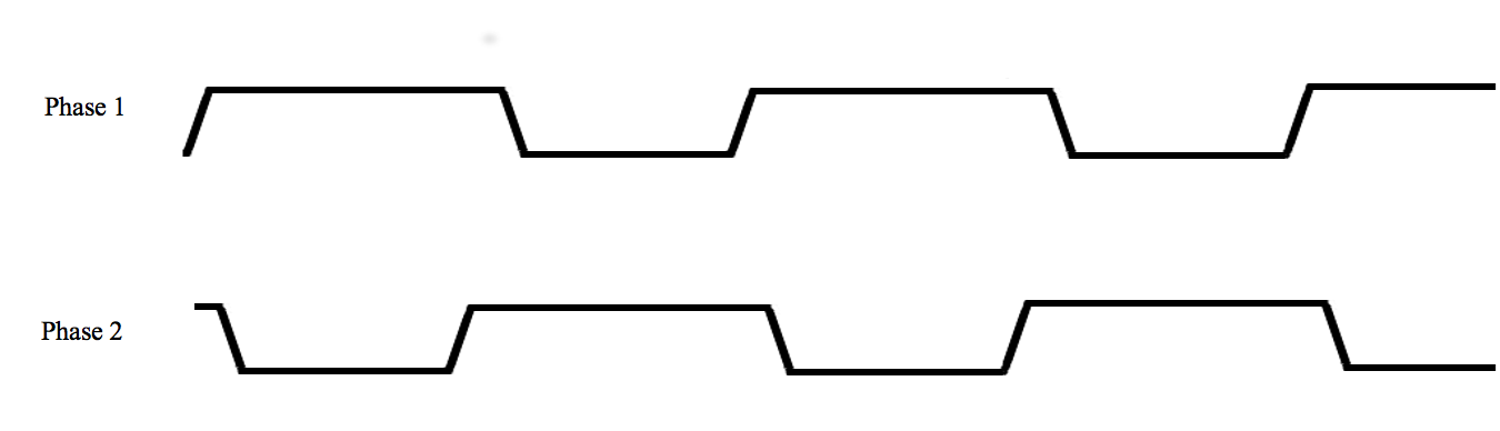
The timing diagram below shows that each of the two phases of the clock are at logic high for a somewhat longer time than they are at logic low. The diagram also shows that the wave forms are not rectangular, as digital waveforms are often drawn for the sake of simplicity. The edges have a non-vertical slope because it takes some time (a minute amout of time) to change from one logic state to another.
In the previous chapter, an edge-triggered latch was describe without a schematic drawing or truth table. Many devices in addition to the edge-triggered latch are edge triggered. They contain a mechanism for detecting a rising edge at its clock pulse input, CP, and capturing the data that is then stable at its input. It then quickly prevents further changes in the input from overwriting the data that was intended to be captured. Such a device is equivalent to the following:
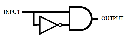
The above figure diagrams a unit that utilizes the propagation delay of a NOT gate (an inverter). For a short time after the input changes from low to high, both inputs to the AND gate are high and therefore the output of the AND gate is high. After the duration of the inverter's propagation delay, the output of the inverter is low and the output of the AND gate is low. Here is a timing diagram:
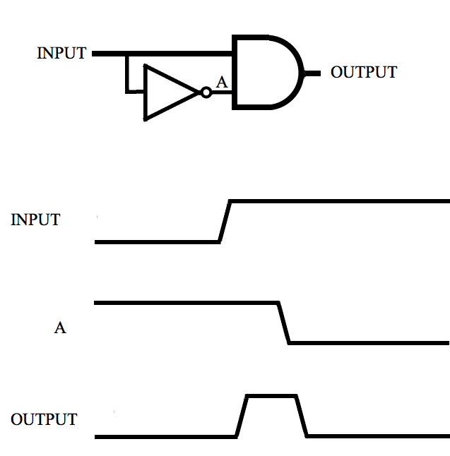
The input and the output are initially low. Point A is initially high. When the input becomes high, A becomes low after a propagation delay. This causes the output to become low. This kind of action is necessary to capture the existing input without allowing changes in that input to have any influence thereafter. An edge-triggered input depends on a source of time delay to temporarily satisfy the requirements of a logic gate input.
The following diagram includes latches that are each gated by Phase 1 or Phase 2 of the microprocessor's clock. This enforces certain timing relationships among the functional units. The functionality that it illustrates still lacks several capabilities that are required to execute useful programs. Nonetheless, a detailed understanding of it is essential.
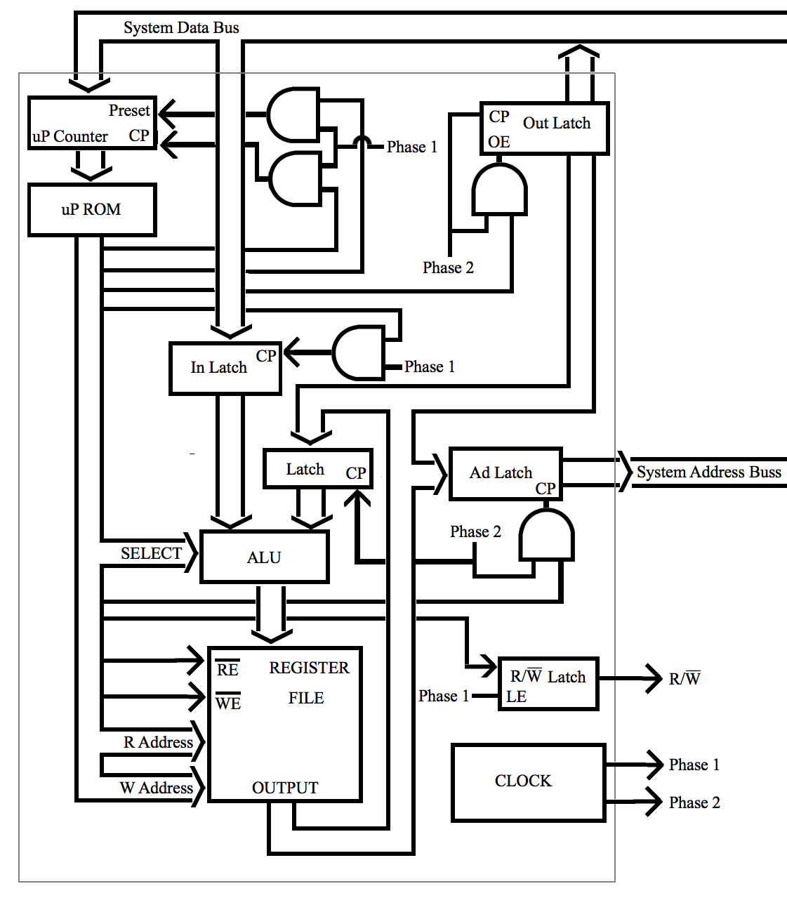
A thin line in the figure separates the microprocessor from the rest of the system. Above the thin line the system data bus is shown. In this example, the system data bus is the source of instructions loaded into the Program Counter.
The address input of the uP ROM is changed upon the rising edge of each cycle of Phase 1. It either changes to an entirely new address (the first of possibly several microinstructions designed to implement a system instruction) or it advances by one microinstruction address in the process of implementing a system instruction.
Typically the last of a series of microinstructions causes a new system instruction to be loaded into the uP Counter from the system data bus.
The diagram illustrates a means of writing on the system data bus and providing the sole source of address bus numbers through the address latch (Ad Latch). It also provides a one-bit latch (R/W Latch) to indicate to the system whether it is reading from it or writing to it (never both at any given time). Timing signals from the clock are also provided to the system.
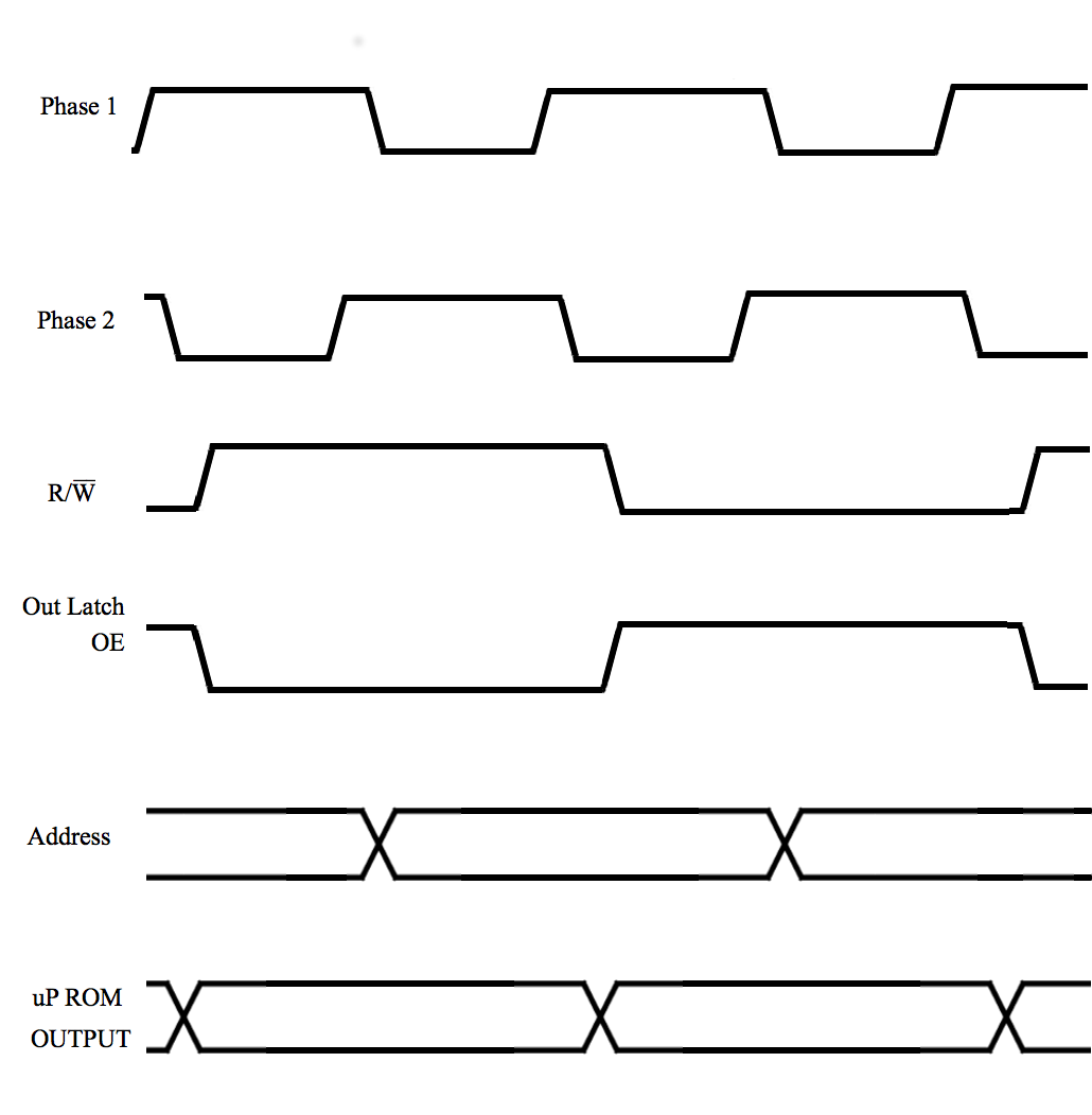
The one-bit latch that indicates to the system the choice between reading from the system and writing to the system is unique in this example as a one-bit latch, and it is also unique because it is updated by a logic high signal. The others are updated by the rising edge of either Phase 1 or Phase 2. When Phase 1 is high, the read write latch is loaded. When Phase 1 goes low, the output of this one-bit latch is remains unchanged.
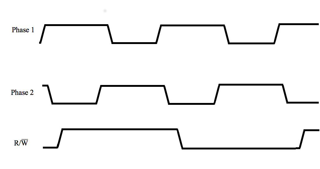
Notice that the onset of a read cycle (when the read/write signal is goes high) is slightly delayed relative to the rising edge of Phase 1. There is an equal amount of delay between the onset of a write cycle (when the read/write signal is goes low) and the rising edge of Phase 1. If a read cycle follows another read cycle, the read/write signal stays high without interruption. If a write cycle follows another write cycle, the read/write signal stays low without interruption.
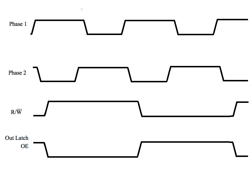
The output latch (Out Latch) is the only latch in this example having tri-state outputs. The output is off while the microprocessor is reading from the system (loading an instruction or loading data into the input latch (In Latch). The output of the Out Latch is always off whenever the read/write signal is high (whenever the microprocessor is reading from the system data bus).
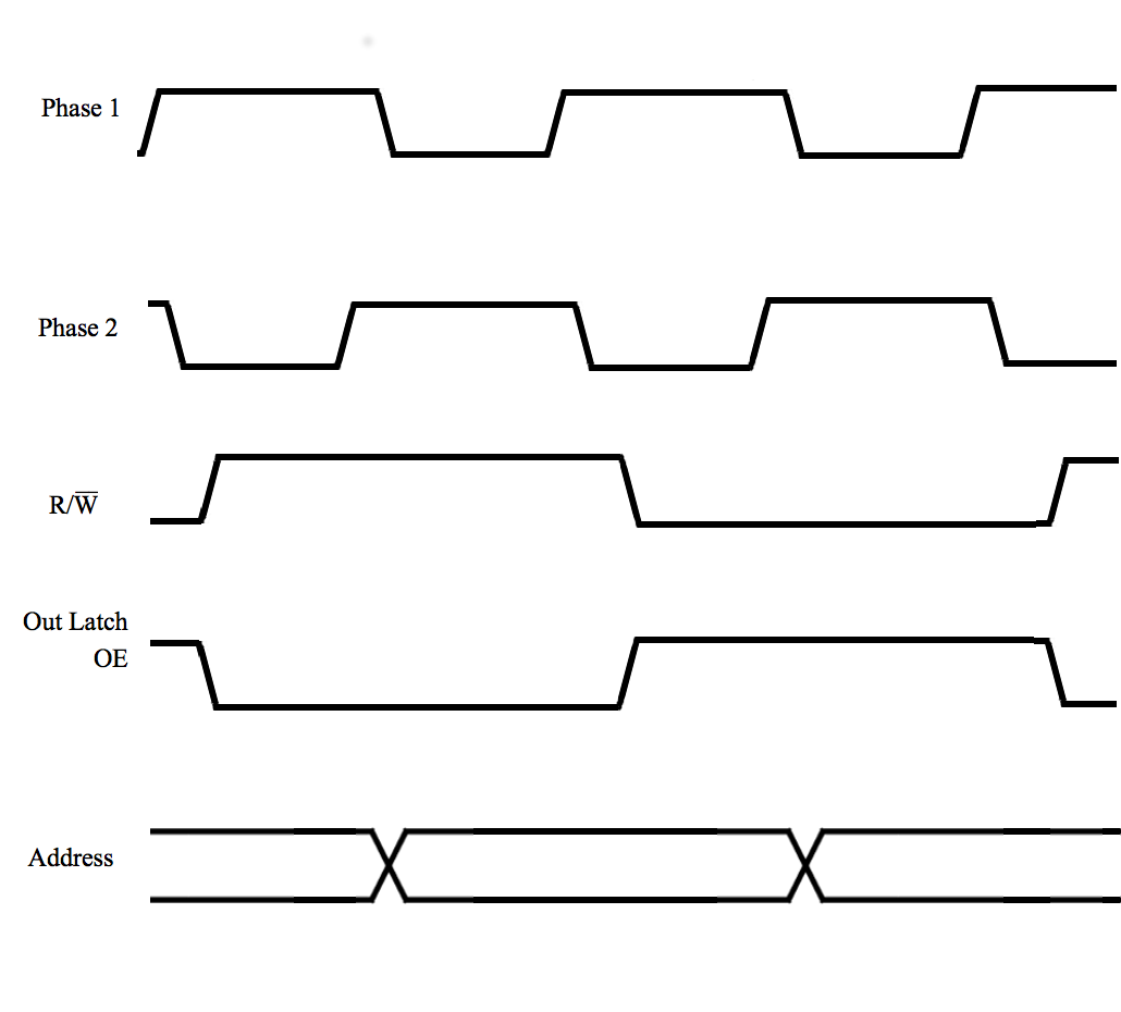
The timing diagram below shows where in the cycle addresses change. They are shortly after the rising edge of Phase 2. Consider a read cycle. Beginning with the address change, the output of the output latch is off, the state of the read/write signal becomes high, and Phase 2 is still high when the rising edge of Phase 1 captures the data on the system bus either (either by the In Latch or the uP Counter). After the next address change, there is a similar sequence of events that writes data onto the system bus.
Consider the write cycle. Beginning with the address change, the read/write signal is low while the output of the output latch is active, and Phase 2 is still high when the rising edge of Phase 1 cause system hardware to capture data.
The timing diagram below shows where in the cycle the output of the microprogram ROM changes.
Contact
https://www.futurebeacon.com/jamesadrian.htm