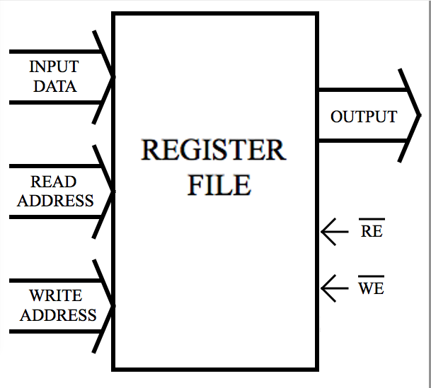
A register file can read any register while writing into any other register.
A signal called read enable allows the register file to acknowledge the read address and send data to the output. A signal called write enable allows the register file to acknowledge the write address and send the input data to the register located at the write address.
When a word such a Preset or an abbreviation such as WE or RE has a bar over it in a diagram, it is called Preset bar or write enable bar or read enable bar as the case may be. This notation and terminology indicates that the signal is an active low signal. lacking such a bar, the signal is presumed to be an active high signal.
Modifying the registers in the register file requires connections to other functional units. The figure below diagrams the sources of data and control signals for the operation of the register file:
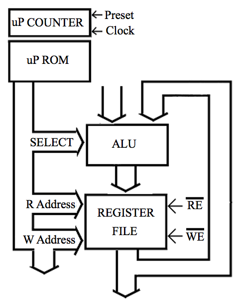
The uP ROM output selects the functions to be performed by the ALU and the register file. As indicated by the arrow in the lower left corner of the figure, some connections of the uP ROM output are not shown. These signals include the Preset input to the uP Counter, and the read enable and write enable to the register file. They are three of the outputs of the uP ROM.
Notice that one of the two sources of data for the input of the ALU is not specified, and the carry output and zero result output of the ALU are not shown. The destinations of the output of the register file is also not included.
The output of the uP ROM does not include the clock signal to the uP Counter. Additional units and diagrams will be required to explain timing. The device diagrammed in the figure above would not work because the timing issues have not yet been addressed.
A collection of parallel signals is typically shown as a wide path terminating in an arrow point. Such a path is called a data bus, or an address bus, or a control bus, depending on its purpose.
There are register files that have the ability to write into a register while simultaneously reading from two other registers. They would have two independent read address inputs and separate read enable inputs along with the write enable and write address inputs.
Contact
https://www.futurebeacon.com/jamesadrian.htm