Microprocessor Design
Back To Introduction
Back To Introduction
Indentation areas (like the one at the start of this paragraph) are links to Google. This allows you to conveniently search for any unfamiliar words or phrases by copying the text in question and clicking on an indentation.
The most basic and widely used means of implementing a sequence of events at the heart of a microprocessor employs a Read-Only Memory (ROM) and a counter which is attached to the address inputs of that memory. The clock input of the counter advances the output number of the counter to step through a sequence of addresses in the ROM. This produces a sequence of parallel outputs at the output of that memory. This read-only memory is called the microprogram memory or the microprogram ROM. It may also be called a uP ROM.
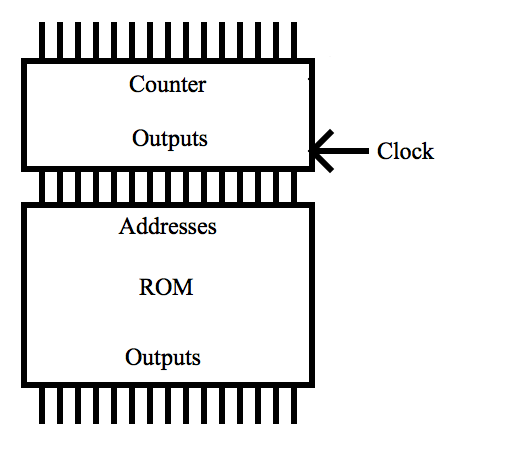
The figure above shows only a few connections between the output of the counter and the address input of the memory. Normally, the number would be much greater. This number is not necessarily equal to the number of ROM outputs. These outputs are connected to the inputs of logic gates that control the behavior of the microprocessor.
This uP ROM is called a microprogram memory because its contents constitute a small and never changing program.
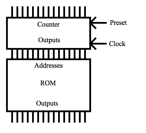
The units in the figure above include a presettable counter. This kind of counter has a number of data line inputs equal to the number of output lines of the counter, and also has a Preset input. If the Preset input is in its active state (this can be either logic low or logic high) the data inputs of the counter are transferred to the output of the counter.
The purpose of the this functional unit is to change the state of potentially very many logic gates within the microprocessor in sequences that correspond to some number of contiguous addresses in the microprogram memory. The sequences can be many distinct sequences. This is because the logic gates being controlled by the output lines of the microprogram memory can cause the Preset input to the counter to initiate a change of address in the memory. The input data of the counter is actually the binary code of a computer system instruction written by a programmer of the computer that has the microprocessor as its central processing unit. System instructions from the operating system or instructions from an application program may require one or more cycles and therefore one or more microprogram memory cell accesses to complete. Each instruction ends with the counter being preset to another address (the start of another sequence) in microprogram memory.
This basic scheme requires the microprogram ROM to be organized in the following way: Each system instruction (provided by the system outside the microprocessor and then through the counter) starts a sequence beginning at the address which is identically the binary code of the system instruction. The system instruction is implemented by some number of contiguous microprogram memory cell numbers until the last in the sequence causes the next instruction to be loaded into the counter. The instructions used by the programmer of the computer are each an address in the microprogram memory. The memory is partitioned so that each partition of addresses executes an instruction written by the programmer.
The following figure is done in a style that is more suited to illustrating tens or hundreds of connections:
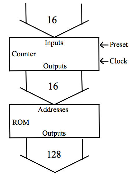
The output at the bottom of the figure is comprised of 128 signals. These signals are connected to the inputs of devices internal to the microprocessor.
 ---------- Microprogram ROM ----------

    Address 	 	 Instruction
   ---------- 	 	 ------------
   0000000001 	 	     A-1
   0000000010 	 	     A-2
   0000000011 	 	     A-3
   0000000101 	 	     B-1
   0000000110 	 	     B-2
   0000000111 	 	     B-3
   0000000111 	 	     B-4
   0000000111 	 	     C-1
   0000000111 	 	     C-2
   0000001000 	 	     .
   0000001010 	 	     .
   0000001011 	 	     .
   0000001100 	 	     .
        . 	 	     .
        . 	 	     .
        . 	 	     .
   11111111100 	 	     L-1
   11111111101 	 	     L-2
   11111111110 	 	     L-3
   11111111111 	 	     L-4

 -------------------------------------
The table above depicts the contents of microprogram memory by associating addresses with microinstructions. The external system or application instruction labeled A is implemented by three microinstructions labeled A-1, A-2, and A-3. Three clock cycles (three advances of the presettable counter) are required to complete this instruction. The instruction labeled B requires four microinstructions. The first two microinstructions of instruction C are shown. There are about 1000 microinstructions in this depiction, but the number of instructions to the microprocessor (external instructions) that the application programmer or system programmer specifies are fewer. Each lettered instruction ends with a microinstruction that causes the next external instruction to be loaded into the presettable counter. Thereafter, the counter output number is incremented by 1 upon each clock cycle until the microinstructions for that lettered external instruction is completed.
The instructions of external programs (system programs and application programs) are moved, each in turn, to the input of the presettable counter, thereby selecting the starting address of a range of microinstructions. The counter advances with each clock cycle until the outputs of the microprogram ROM cause the microprocessor to load another instruction from the external program.
The microprogram in the microprogram memory is comprised of microinstructions. These microinstructions each provide the output signals that control the logic gates internal to the microprocessor.
The presettable counter that determines the address inputs of the microprogram memory obtains its input from a program stored outside of the microprocessor. This counter is called the microprogram counter. It may also be called the uP Counter.
Contact https://www.futurebeacon.com/jamesadrian.htm