Access to instructions independent of the rest of the system offers an advantage beyond simultaneous accesses. It allows the width of instruction memory and the width of system memory to be different. This has given rise to the Very Long Instruction Word (VLIW) approach to instructions and program storage.
VLIW instructions are divided into fields. Fields are subsets of the long instruction word. These fields can be used to control separate functions within the microprocessor. Propagation delays are reduced as compared with the microprogram-ROM-with-microprogram-counter method.
In a VLIW design, The terms data memory and system memory and system have been used to distinguish the system address space from instruction memory or program memory.
Using a very long instruction word is a technique intended to reduce the time needed to execute programs. This is very much associated with the effort to reduce (to one clock cycle where possible) the time required to execute each instruction. One-clock-cycle instructions are also characteristic of Reduced Instruction Set Computing (RISC). The preexisting alternative to RISC has come to be called Complex Instruction Set Computing (CISC). A VLIW design may use one-clock-cycle instructions or not. This, in itself, does not make it a RISC design or a CISC design.
The fields of a very long instruction word serve as the source of control signals for the various functional units in the microprocessor. Here is a hypothetical set of fields:
-----------------------------------------------------------------------
| ALU/Shifter | Register file | Latches and Buffers | Branching Logic |
|  12 Bits    |    30 Bits    |      10 Bits        |      5 Bits     |
-----------------------------------------------------------------------
There is also the matter of the timing of these control signals to enable functions. Timing logic must gate the bits in these fields before they are used as control signals. The ALU/Barrel Shifter could receive all of its control signals at the same time, but that could not be the case for the whole collection of latches and buffers.
The timing logic needs to either contain a multi-phase clock or receive signals from such a clock. These signals are used by the timing logic to assure that control signals change at the right times.
To simplify the instruction decoder, it is desirable for the long instruction words to have the same number of fields having the same size and the same order; but many instructions need not include a field for every possible function. For example, non-branching instructions need not have a field for the branching logic. This is remedied if each field has a no-operation code. If there are 7 meaningful codes for selecting a bit from the processor status register, and one of 8 possibilities of a 3-bit field does nothing, that field can be in every instruction word. Likewise, there is a code in the barrel shifter that allows the data to pass through unmodified. Also, there are logical operations in the ALU which which leave its input unchanged. In any given instruction, the register file write enable does not need to be active. Because fields can be made inactive or go unused, it is possible to define the fields of the long instructions uniformly.
In many VLIW designs, the very long instruction word delivers more than one instruction to the microprocessor. The distinction between a long instruction word and an instruction contained within a VLIW is greatly aided by using the term op code when referring to an instruction within the VLIW.
In the case where the VLIW delivers more than one op code, the instruction decoding process must select and schedule the implementation of each op code. This is not the case in the following illustration:
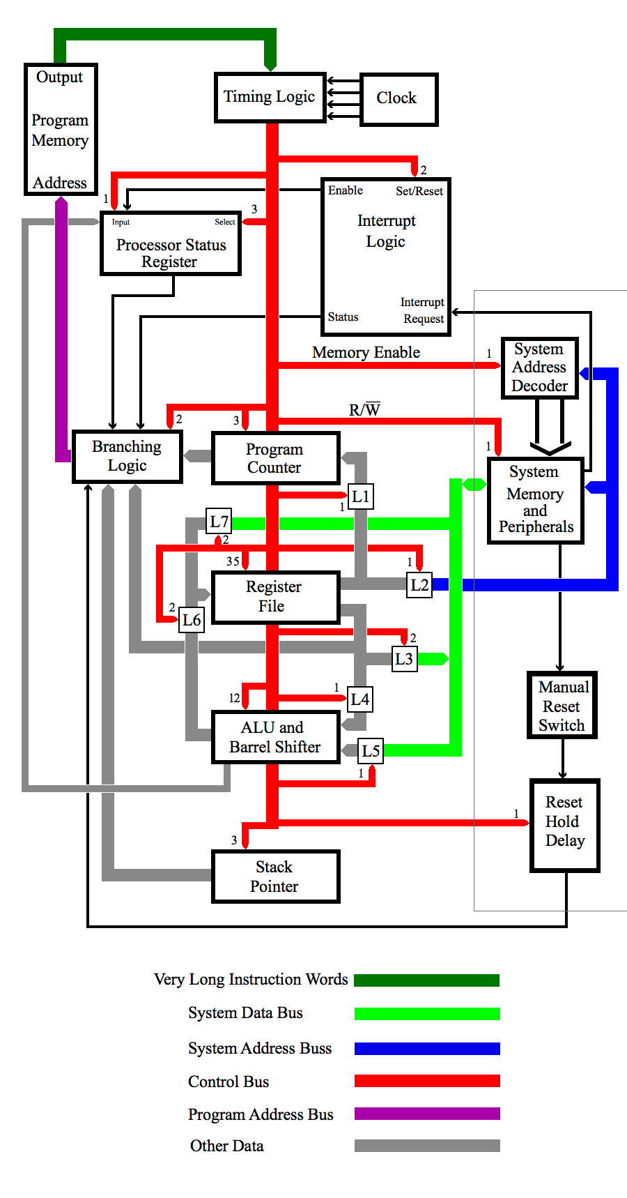
In the diagram above, L1 through L7 are edge-triggered latches. L1, L2, L4, and L5 are each alone in writing to there output destination. This allows their outputs to be perpetually enabled. L6 and L7 must not write to the register file at the same time. To prevent this, they have tri-state outputs and are enabled one at a time. L3 must not write to the system data bus while data is coming in from the system, so L3 must also have tri-state outputs.
The register file has two outputs. One of them provides data to L1 and L2 while the other output provides data to L3, L4 and the branching logic.
The number of control-bus signals connected to each unit is shown next to the red arrow in each case. The program counter has three (reset, present, and a clock pulse for advancing the address number). The ALU/Barrel Shifter has 12. The register file has 35. The stack pointer has 3 (reset, present, and clock pulse). Each latch has either one or two control signals (one if perpetually enabled and two if not). If a latch has two control signals, the timing of those signals may or may not be simultaneous.
The functionality depicted in the diagram implies the size and number of the fields in the VLIW. It also forms a framework for defining an instruction set and the timing required to implement instructions.
Notice that, if a branch instruction is to be done in one clock cycle, that branch can be taken only on the basis of the settings of the processor status register prior to the execution of that branch instruction.
The status output of the interrupt logic is active only when the system is holding active an interrupt request, and the most recent update of the set/reset input is a set (as opposed to a reset). This set/reset input is controlled by two bits of the VLIW. When this field is 00, set/reset is unchanged. When this field is 11, the setting is also unchanged. When the field is 01, the permission to process an interrupt is set. When the field is 10, the permission is reset. When reset, the status output is inactive and so is the enable bit which updates the processor status register.
The branching logic saves (latches) address words from the program counter, the register file, and the stack pointer. It also has a permanent storage of two vectors not shown. They are the reset vector and the interrupt vector. The output of the branching logic is the exclusive source of the program address. The reset vector is used when the signal from the reset hold delay unit is active. The interrupt vector is used when both the status and processor status register inputs are active. Otherwise, one of the first-mentioned three addresses is chosen by two bits from the control bus.
The value that this design presents is its framework for the design of an instruction set. One must discern all of the one-clock-cycle instructions made possible by this illustration and the timing required for each of them. This is an exercise that must be undertaken frequently. Later, you can take on the opposite task - designing a microprocessor for a given instruction set. There are a lot of observations to be made working in each of these directions.
An inherent characteristic that motivates the design of other variations on the original Harvard Architecture is its inability to update program memory with instructions from system memory or system peripheral devices. That capability could be added while still using very long instruction words. Program memory would need to become read/write memory instead of read-only memory. A read/write input would be required. The output bus from the program memory would need to be extended to the system/peripheral memory data bus with a latch or buffer capable of separating the two.
Previously, accesses to the system were called read cycles and and write cycles. It is now just as common to call read cycles load cycles while calling write cycles store cycles. As software commands, they are often called load commands and store commands.
The illustration above diagrams a four-phase clock. Very often, internal functional units have no more than one-fourth of the propagation delay of system memory accesses, thereby allowing a succession of events during one clock cycle.
If rising-edge-triggered latches are used to capture data from one bus in order to write data onto another bus, there is a motive to create clock phases that are at logic high longer than they are a logic low. When a latch captures data at the beginning of a phase from a bus that changes at the end of another phase, there needs to be a hold time between the logic high of the ending phase and the rising edge of the phase that is just beginning. This assures that the latch will be capturing stable data.
One is free to design the timing logic in such a way that a unit enabled on the rising edge of one phase could be disabled upon either edge of any other phase.
Where latches or buffers separate functional units within the microprocessor, and the clock provides more than one phase, it is very often possible to start a new op code before another is finished in designs that have more than one op code in each VLIW. This is called pipelining.
Contact
https://www.futurebeacon.com/jamesadrian.htm