A microprocessor typically contains functional units such as memories, registers, latches, counters, multiplexers, arithmetic and logic units, and others. These are combined to form a microprocessor.
Logic gates produce only one output, and may have more than one input. The output may be connected to the inputs of several other devices.
Except when in transition, any input or output of a logic gate, whether electronic or optical, is either at a low voltage or intensity or a higher one. The characterizations high and low are historical. For purposes of logic, they could just as well be any two states of any kind. They could be a polarization right or left or anything else. Regardless of the underlying technology, these two states are and shall be called logic low and logic high.
Because there are exactly two states of interest, the term binary is used to characterize logic gates and digital devices. A logic high is often referred to as 1 whereas a logic low is then referred to as as 0. A number or a digit within a number that is either 1 or 0 is called a bit. Sets of such bits form binary coded numbers. Although is it possible to make three-state or multi-state devices, the term digital has been widely intended to mean binary digital.
Groups of binary outputs often form what is intended to be interpreted as a number. An example of the most widespread binary notation is diagramed below:
bit 7 | bit 6 | bit 5 | bit 4 | bit 3 | bit 2 | bit 1 | bit 0 |
There are 8 bits in this number and in such a case the number is called a byte. More typically, a byte is notated as something like the following:
a7, a6, a5, a4, a3, a2, a1, a0

or

b7, b6, b5, b4, b3, b2, b1, b0
The letter indicates which byte and the number indicates which bit of that byte. A specific byte might be, for example, 10101100.
The code that associates such bytes with numbers takes advantage of the placement of bits, left to right, to form a sum. Bit 0 may be either a 1 or a 0, as is the case for each of the other bits, but bit 0 means that either 1 or 0 is added to the sum while bit 1 means that either 2 or 0 is added to the sum. Each advance to the left in the written number represents a more significant bit in that the value added to the sum is twice that of its neighbor on its right. The example byte above equals 128 + 32 + 16 + 8, which equals 184. A byte comprised of all 1's would equal 128 + 64 + 32 + 16 + 8 + 4 + 2 + 1, which equals 255.
Logic gates and the logical operations they perform must be understood by means of truth tables. The following symbols are commonly used in schematic drawings. Under each logic gate symbol there is a truth table indicating the output associated with the shown input.
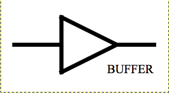
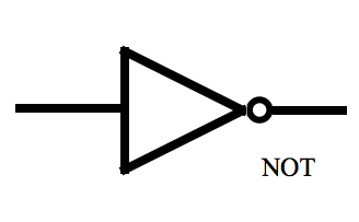
    BUFFER IN    BUFFER OUT         NOT IN    NOT OUT
    -----------------------         -----------------
        0            0                 0        1
        1            1                 1        0
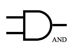
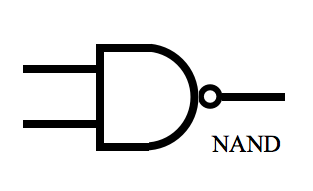
      A      B    A AND B          A     B   A NAND B
     ---------------------        --------------------
      0      0       0             0     0      1
      0      1       0             0     1      1
      1      0       0             1     0      1
      1      1       1             1     1      0
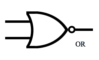
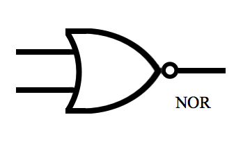
      A      B     A OR B          A     B    A NOR B
     ---------------------        --------------------
      0      0       0             0     0      1
      0      1       1             0     1      0
      1      0       1             1     0      0
      1      1       1             1     1      0
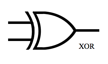
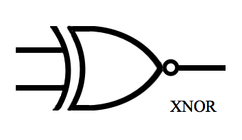
      A      B     A XOR B          A     B    A XNOR B
     ----------------------        --------------------
      0      0       0              0     0       1
      0      1       1              0     1       0
      1      0       1              1     0       0
      1      1       0              1     1       1
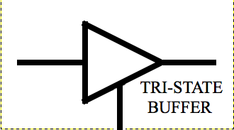
      TRISTATE INPUT     DATA IN      DATA OUT
     ------------------------------------------
           0                0         No Output
           0                1         No Output
           1                0            0
           1                1            1
The NOT gate is also called an inverter. If an input of of an inverter is called A, its output can be called A' (pronounce A prime). This means that if A is 1, then A' is 0; and if A is 0, then A' is 1. A' is said to be the complement of A, and A is said to be the complement of A'.
The Buffer in the first figure with a truth table amplifies a signal without changing its meaning.
The vertical line at the bottom center of the figure depicting the tri-state buffer is tristate control input. When it is active, the output of the buffer is off and does not produce and output. This allows another tri-state output to be connected to its output without conflict. Tri-state outputs that are connected together require that only one of those is active at any given time.
Notice that the AND operation outputs a 1 only if both inputs are 1. The NAND operation does the opposite. Its output is 0 whenever both inputs are 1, and the output is 1 otherwise. This same sort of naming occurs in the case of the OR operation. The NOR operation produces an out that is exactly opposite of the OR operation. There are also logical operations that simply use one of the inputs as the output, or the complement of an input as the output.
There are also multiple input logic gates that have three or more inputs. For instance, a five-input AND gate requires all five inputs to be 1 in order to produce a 1 as an output; a five-input NAND gate requires all five inputs to be 1 in order to produce a 0 as an output; A multiple-input OR gate produces a 1 if any of its inputs are 1; and, a multiple-input NOR gate produces a 0 if any of its inputs are 1.
The figure below illustrates a function implemented by two logic gates that are connected. It takes as input a single bit from each of two sources, one marked A, and one marked B. It adds them together with an XOR gate, producing a sum. With an AND gate, it also produces a carry bit which is 1 in the event that both A and B are 1. It is called a half adder because it does not accept as input a carry bit from an adjacent adder. A full adder would require more gates.
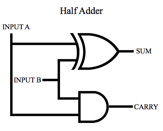
	  10110011
	 +       1
	  --------
	  10110100
The sum for bit 0 in binary is two = 10, so the 0 is written in bit 0 of the sum while the 1 is carried to the next column. A carry it is produced by the full adder associated with bit 1 and then bit 2 produces no carry bit. Each bit other than bit 0 needs to wait for a carry bit input to its full adder.
A logic gate of any known technology will produce a delay between the time that any of its inputs change and the time that its output changes. This phenomenon is called propagation delay.
A decoder is a device that translates a binary code into a selection of one output. An input of 11 will produce output three and that output only. An input of 10 will make the second output active and that output only.
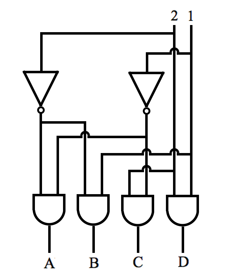
     Bit 2   Bit 1     A     B     C     D
    ---------------------------------------
       0       0       1     0     0     0
       0       1       0     1     0     0
       1       0       0     0     1     0
       1       1       0     0     0     1
Contact
https://www.futurebeacon.com/jamesadrian.htm